
PCB Artwork
From schematic to board layout — multilayer, high-density, impedance-controlled
We take your schematic and turn it into a manufacturable PCB layout. Component placement, routing, power/GND plane design, and impedance-matched high-speed lines are all handled directly by experienced engineers.
- Multilayer board layout (2–8 layers)
- Impedance control · high-speed routing (USB, RF, differential pairs)
- EMI/EMC-aware placement and routing
- Full fabrication data: Gerber, BOM, pick-and-place files
- Seamless follow-up with sample fabrication and assembly
Boards we lay out
Placement and routing rules change with layer count and signal type. Every board is drawn by the same team to the same standard.
- Multilayer · impedance
- 2–8 layers. Stackup first, impedance widths calculated, then routing. Experience with 8-layer PoE switches and gigabit PHY boards.
- High-speed · differential
- USB 3.0, Ethernet, LVDS, MIPI. Pair length matching and continuous reference planes.
- RF · antenna
- 10GHz radar, UWB, patch and horn antenna boards. Ground via fences and feed-line impedance control.
- Power · motor
- 48V electric pump controllers, 6-axis BLDC drivers. Copper width for current paths and heat dissipation designed together.
- High density · compact
- QFN, BGA, 0402. Via-in-pad and fan-out rules matched to fabrication capability.
- Mechanical fit
- Board outline and connector positions from DXF/STEP, placed without interference. Assembly checked in 3D STEP.
Layout gallery
3D views of boards we have designed. Look for a case similar to your board.
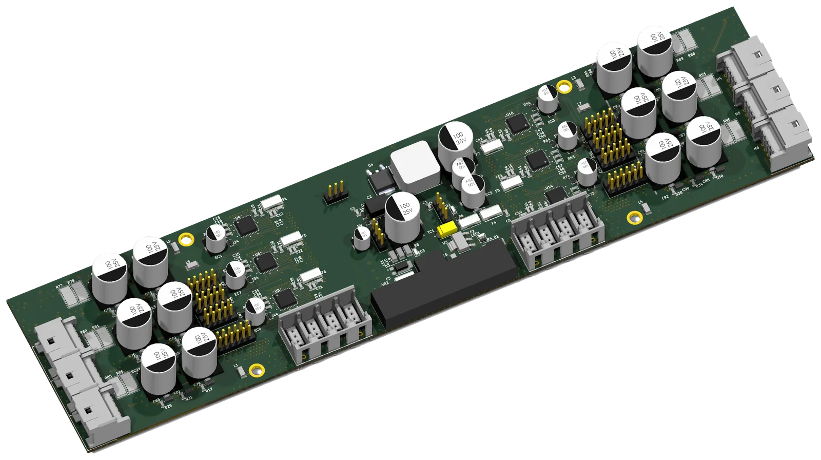
6-channel BLDC motor driver board. 6 driver ICs, 23 electrolytic capacitors.
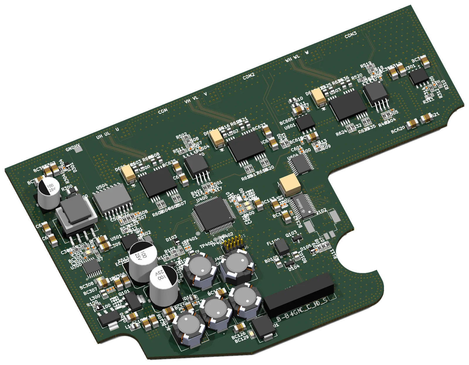
Isolated gate driver and power control board. Optocoupler and power inductor mounted together.
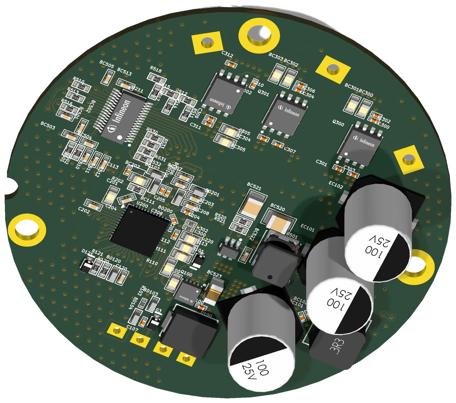
100V-class round motor control board. Gate driver and MCU placed within the round outline.
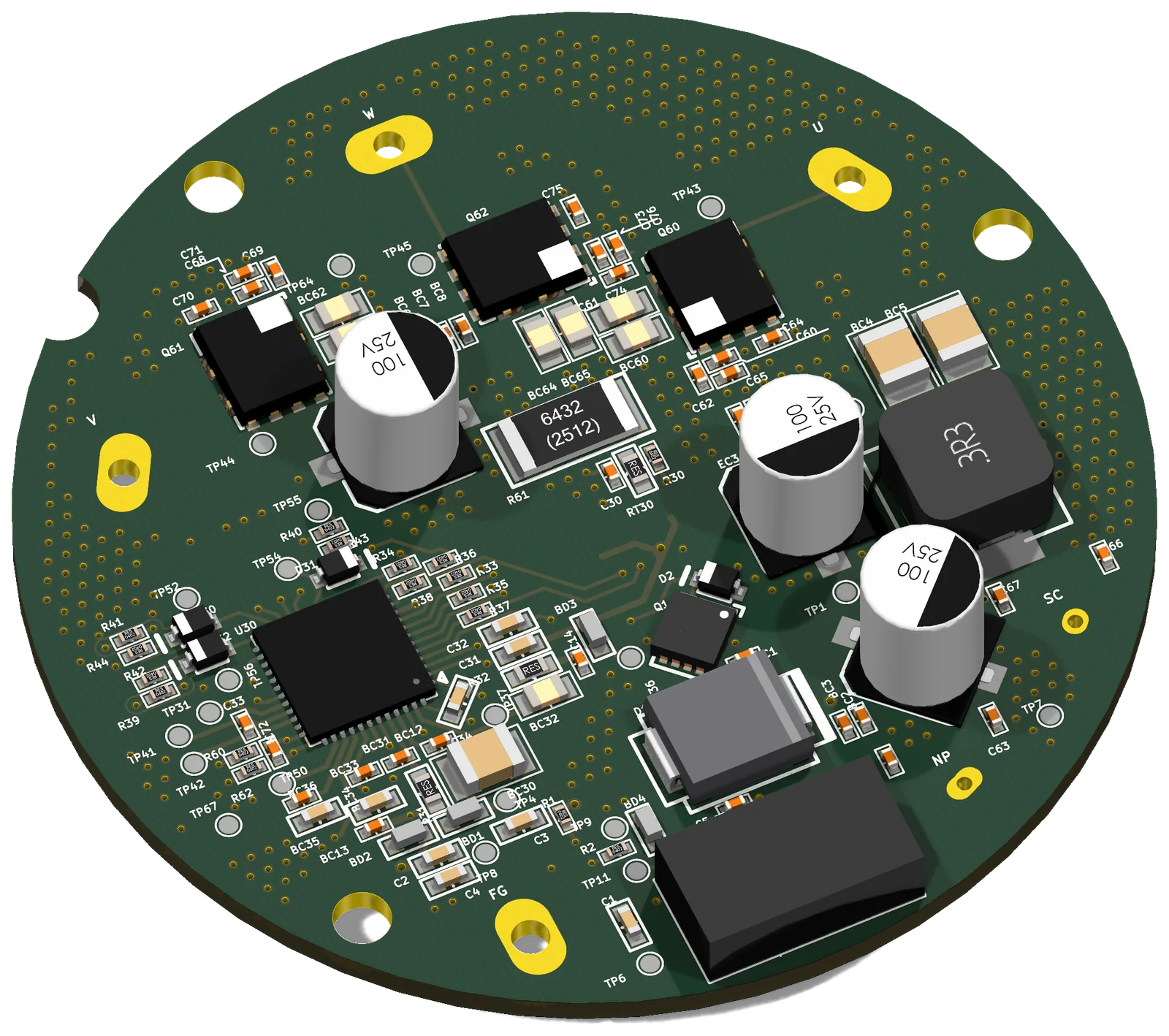
Compact power switching board. 4 MOSFETs and protection diodes.
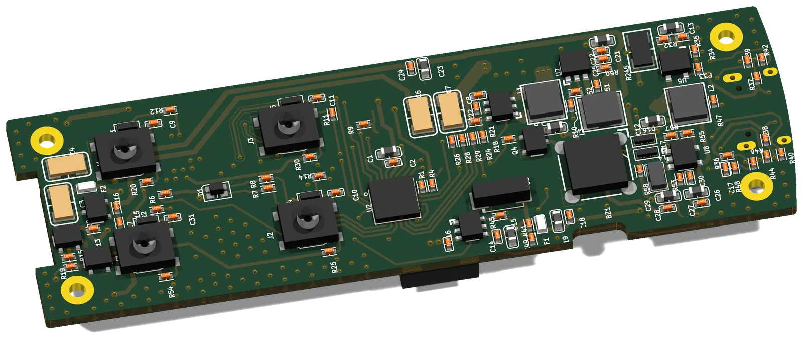
Compact handheld control board with 4 tact switches and USB-C.
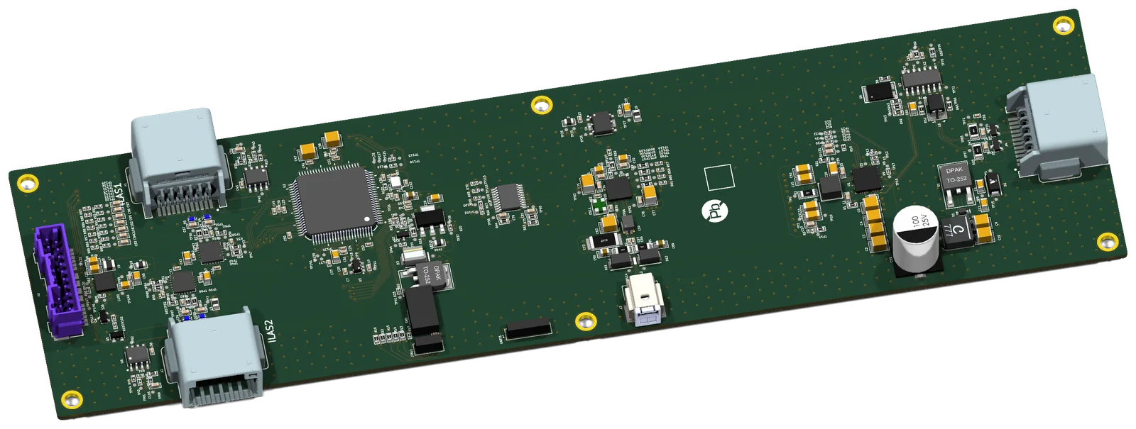
Long automotive control board. CAN transceiver, high-side switches.
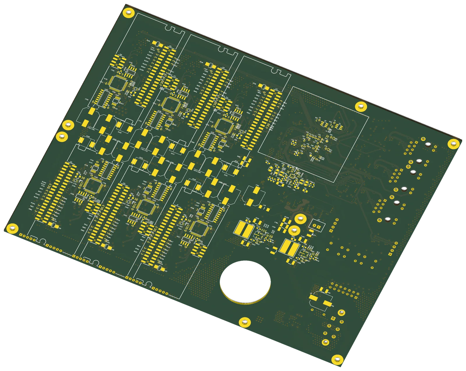
High-density I/O interface board. 30 photocouplers, 12-channel RS-485.
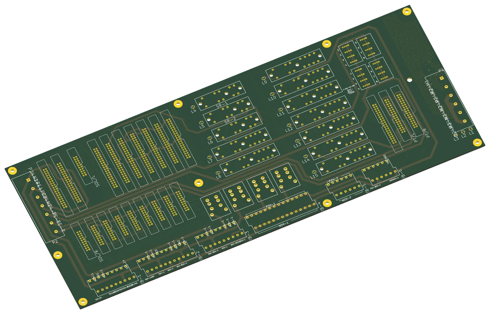
Large relay control board. 79 diodes, safety relays, box-header connectors.
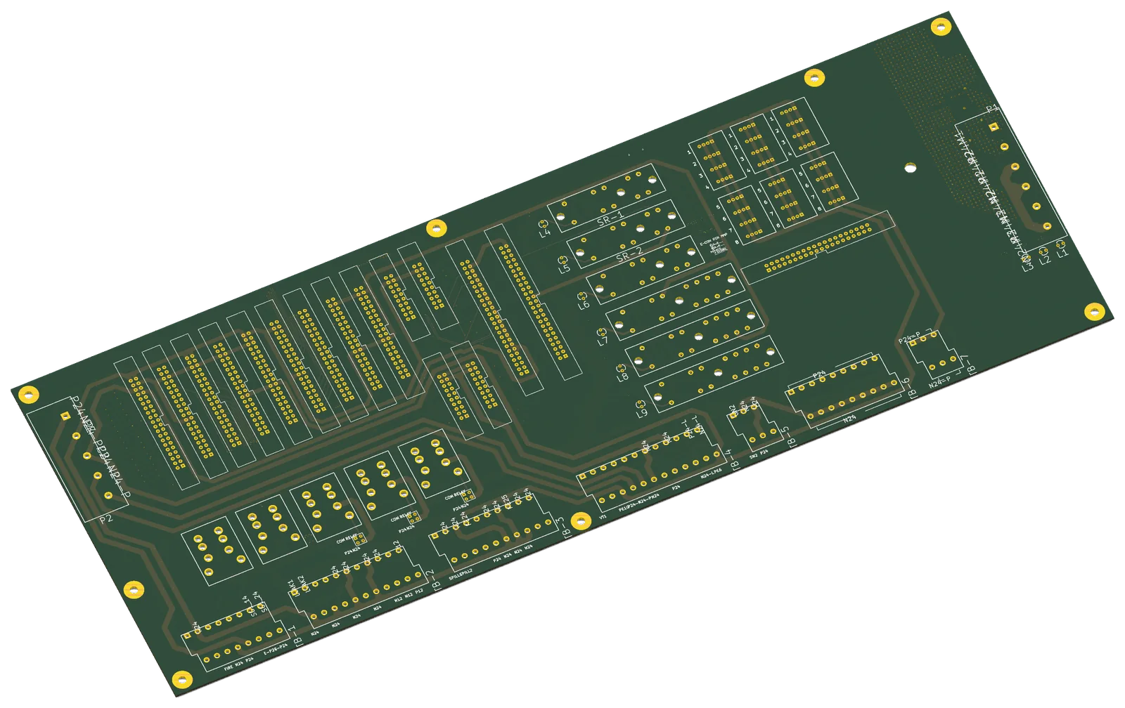
Large relay and terminal block board.
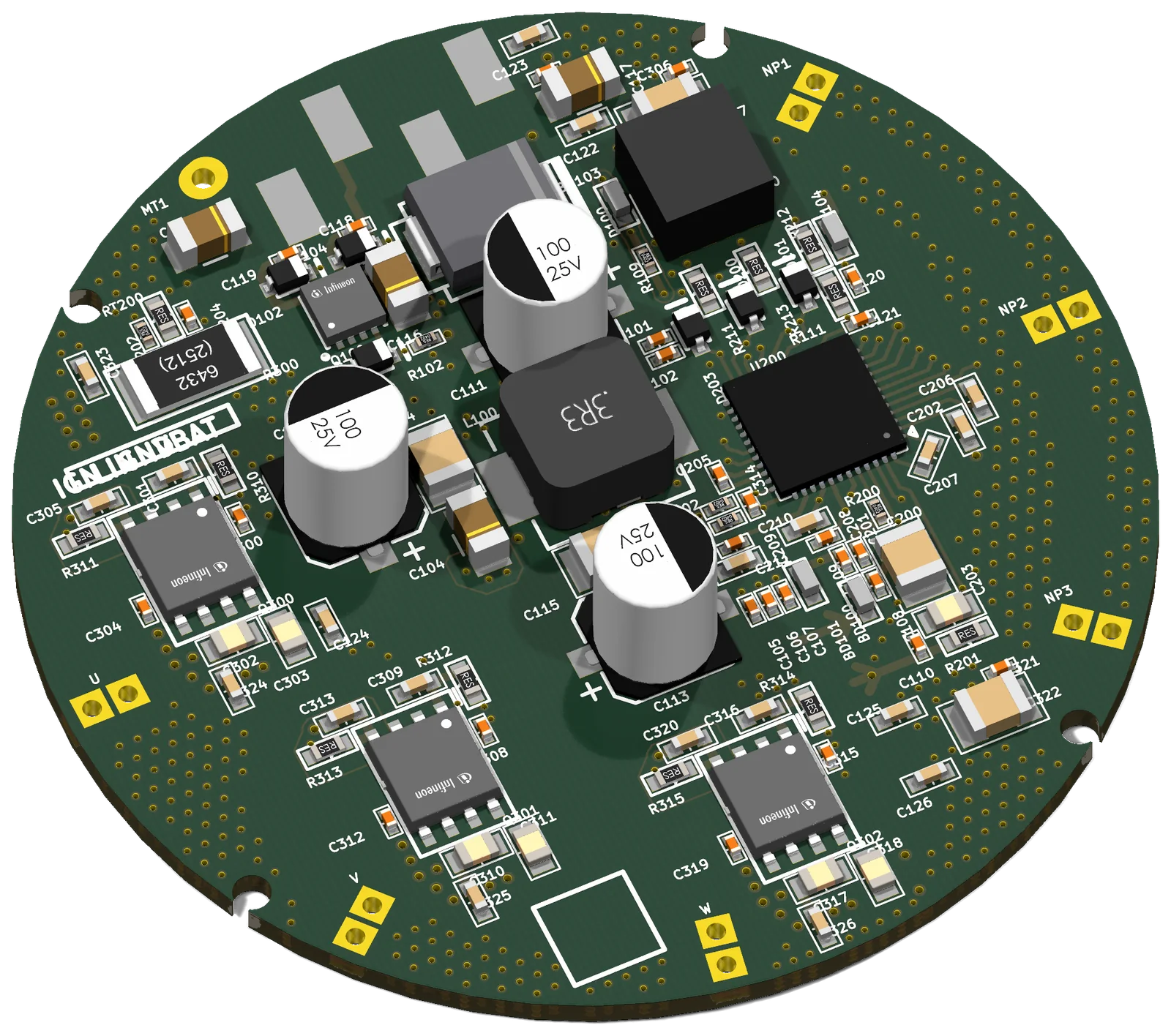
Round motor driver board. 4 MOSFETs, electrolytic capacitors.
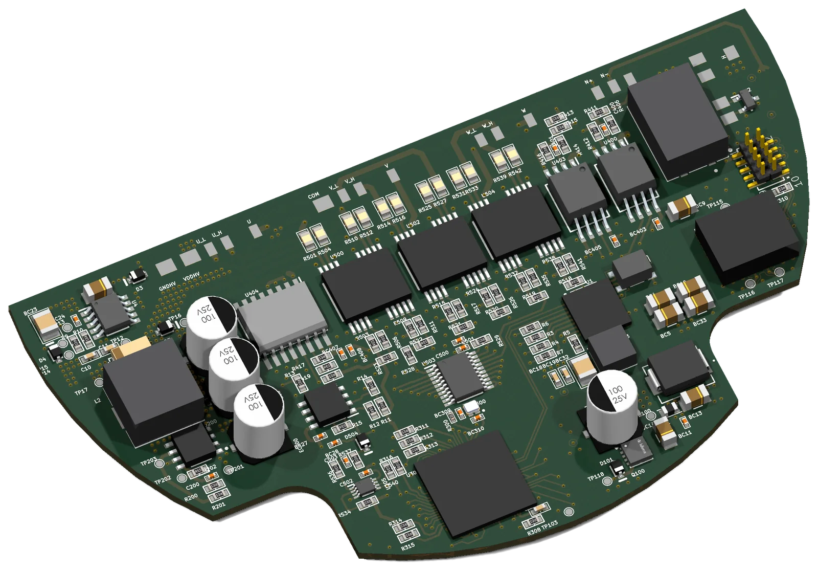
Isolated communication and power board. 3 isolated ICs, EMI filter, power inductor.
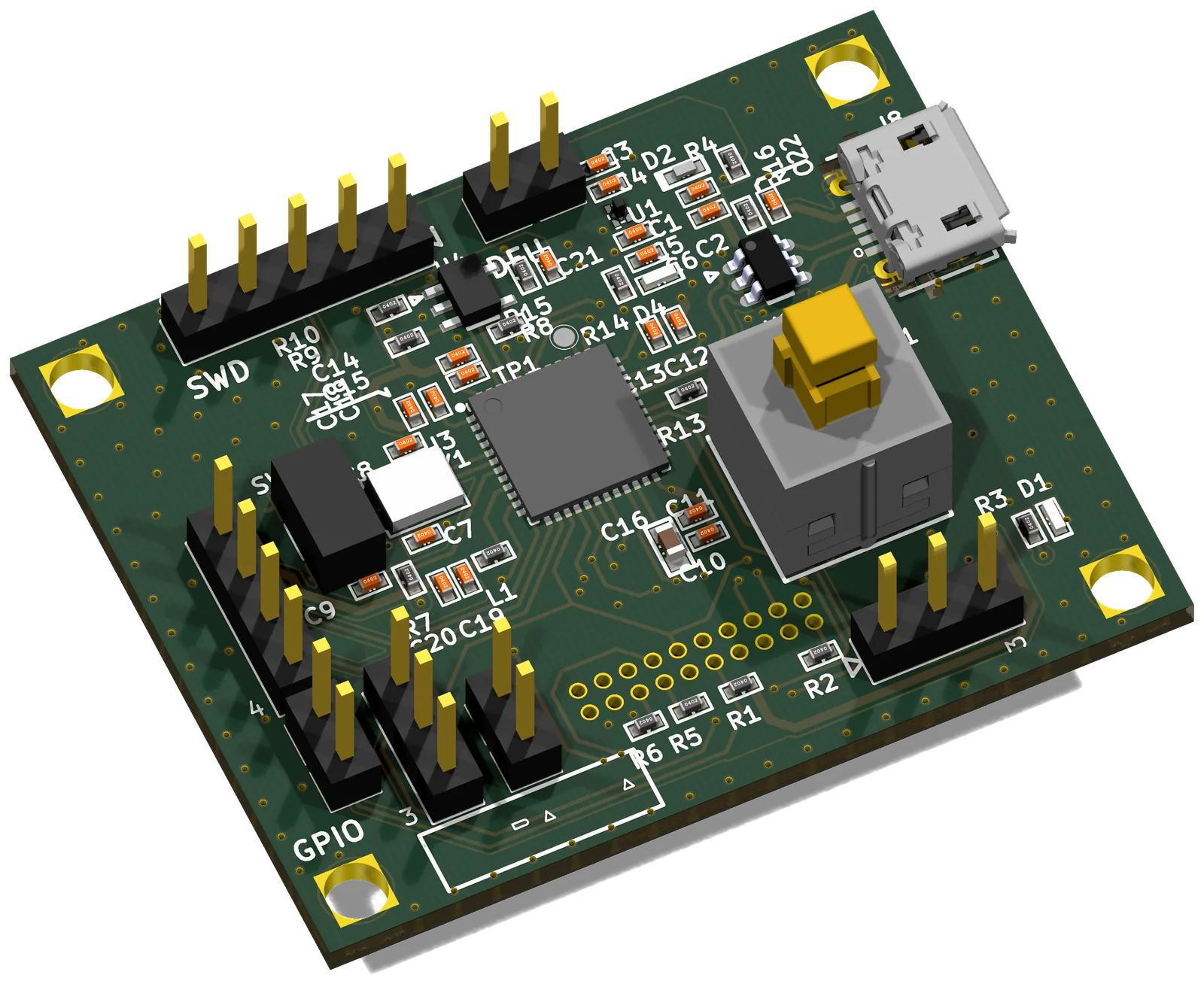
STM32F411 USB development board. SWD/GPIO pin header, micro USB.
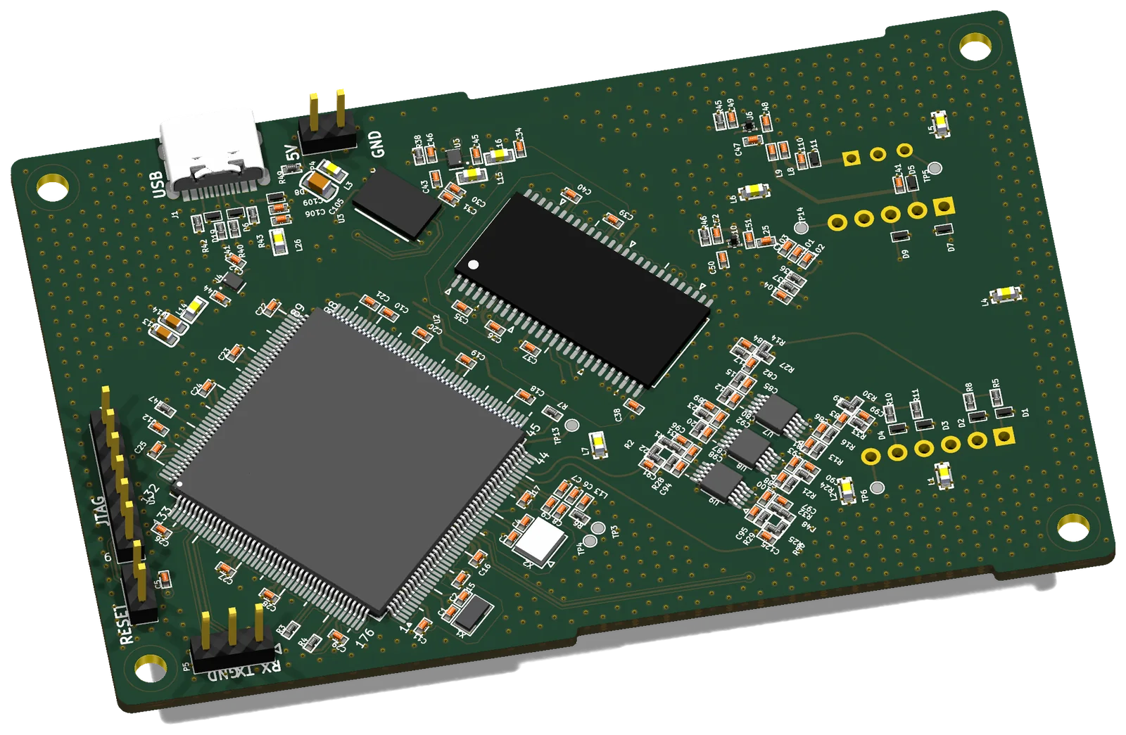
Precision analog measurement board. 3 operational amplifiers, USB-C, JTAG header.
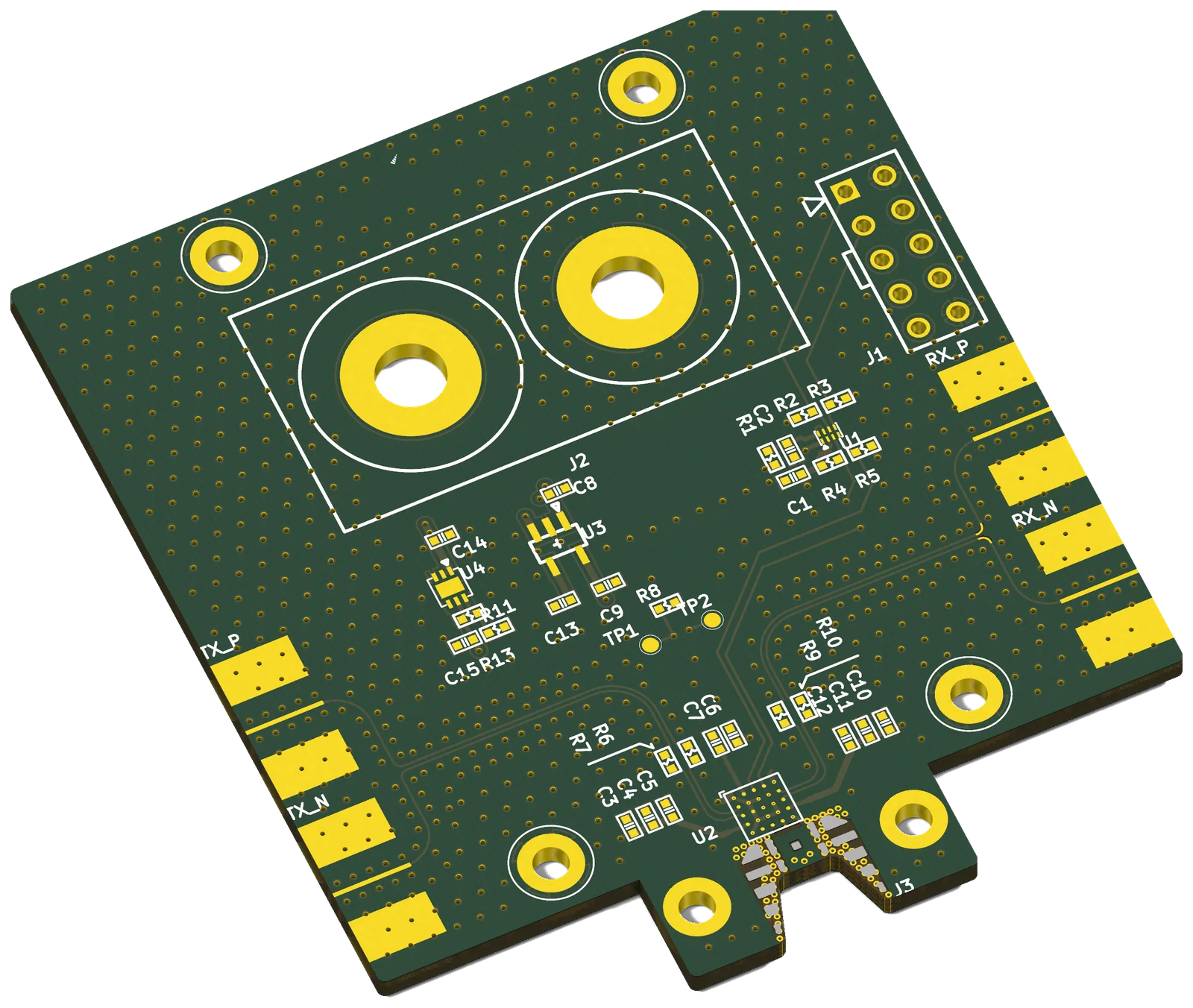
RF antenna board. 4 SMA connectors, onboard antenna pattern.
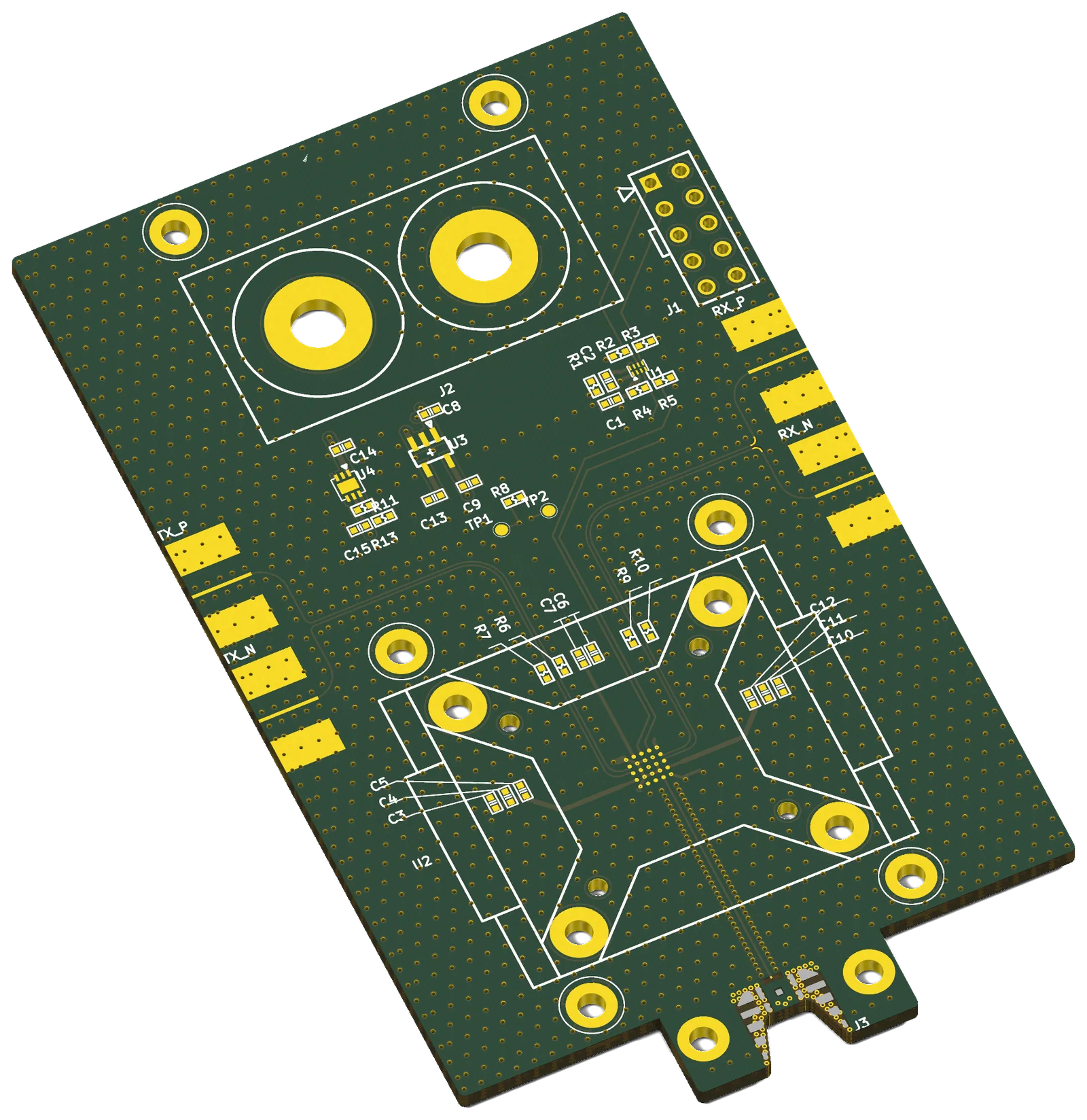
RF antenna board (extended variant). 4 SMA connectors, onboard antenna pattern.
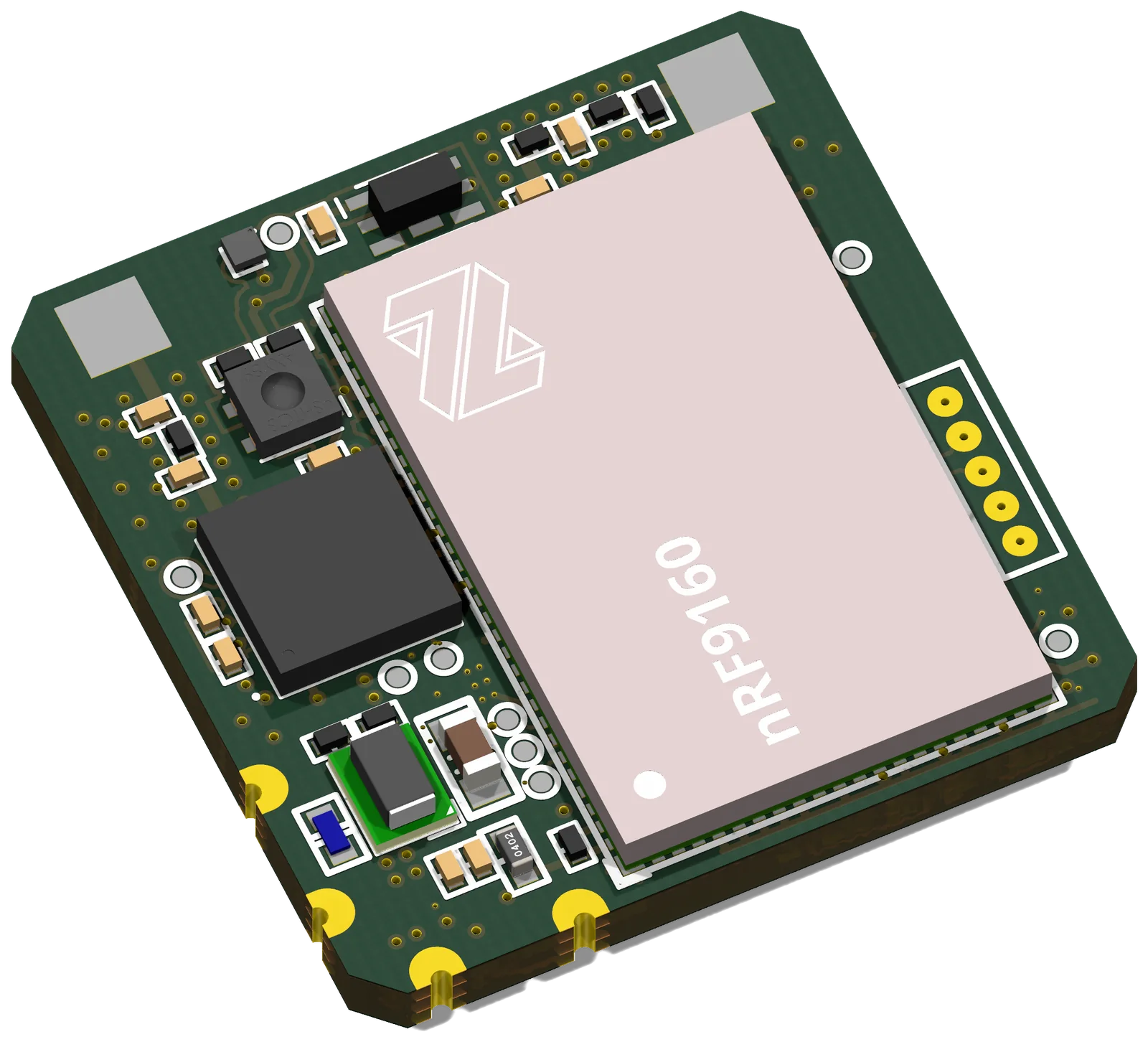
LTE-M/GNSS miniature module board. Accelerometer, light sensor, flash memory.
How it proceeds
- 1Schematic and outline intake
Schematic (any CAD format), mechanical DXF, connector and mounting requirements. Missing part libraries are built from datasheets.
- 2Placement review
You receive a placement drawing first. Mechanical interference, connector orientation and hot parts are settled here.
- 3Routing and planes
Power/GND planes, impedance widths, differential length matching, then DRC clean.
- 4Review notes and delivery
Design review notes and a 3D view are sent together. After sign-off: Gerber, drill, placement data, BOM and assembly drawing.
Deliverables
- Gerber (RS-274X), drill, IPC-356 netlist
- Pick-and-place data, assembly drawing, stencil data
- BOM (orderable part numbers, package, quantity)
- 3D STEP, stackup specification, design review notes
- Native design files (Altium, KiCad or the format you request)
How quoting works
Layout quotes are based on the number of component pins on the board. Upload the schematic to the quote tool and it reads the pin count and shows a price immediately; nothing is charged before confirmation. Special conditions such as impedance, RF or high density are quoted individually after intake.
What speeds things up
- Original schematic file (a PDF is enough to start)
- Mechanical outline DXF or STEP, connector and mounting hole positions
- Preferred layer count, thickness and finish (we propose if unknown)
- List of special signals: impedance targets, differential pairs, RF feeds
Upload your schematic
A pin-count-based estimate appears immediately. No cost before confirmation.
Frequently asked
I only have the schematic as a PDF.
That works. We redraw the schematic from the PDF and deliver that schematic file as well.
Some parts have no library.
We build footprints and 3D models from the datasheet. The libraries are included in the deliverables.
I want to approve placement first.
That is the default. You receive the placement drawing first and routing starts after your confirmation.
Can fabrication and assembly follow?
Directly, from the same data. Ordering fabrication and assembly together skips the Gerber review step.